With the increasing demand for energy, LED with its high efficiency, environmental protection, safety advantages have been rapid development, but LED in the packaging process of pollutants are also confused headaches for a long time, oxide and particle pollutants on the surface of the bracket and chip will reduce product quality, if in the packaging process before dispensing glue, Plasma cleaning before lead bonding and package curing can effectively remove contaminants, while plasma cleaning before scaffold plating can also improve the plating effect.
Principle of plasma surface treatment
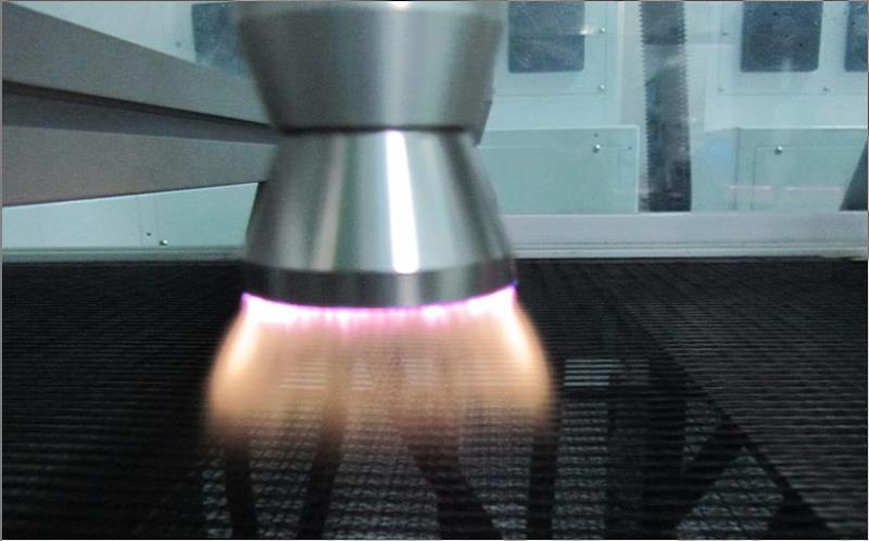
Plasma, also known as the fourth state, is composed of ground state atoms, molecules, excited state atoms, molecules, free electrons, positive and negative ions, atomic groups and photons, which appear objectively neutral. The point particles in the plasma can be treated on the surface of the workpiece through chemical or physical action to achieve the removal of pollutants at the molecular level (generally 3-30nm thickness), thus improving the surface activity of the workpiece. Corresponding to different pollutants, different cleaning processes should be used, according to the selection of different process gases, plasma cleaning is divided into chemical cleaning, physical cleaning and physical chemical cleaning.
Chemical cleaning: Plasma cleaning with chemical reaction as the main surface reaction. For example, hydrogen reacts with organic substances to generate water and volatilize.
Physical cleaning: Plasma cleaning based on physical reaction, also known as sputtering corrosion (SPE). For example, Ar+ is accelerated to generate kinetic energy under the action of self-bias or external bias, and then bombarded on the surface of the cleaned workpiece placed on the negative electrode, which is generally used to remove oxides, epoxy resin spills or particulate pollutants, while carrying out surface energy activation. Physical and chemical cleaning: Both physical and chemical reactions play an important role in surface reactions.
The specific application of plasma surface processor in LED technology
1. The purpose of dispensing is to connect the chip and the bracket, but the pollutants on the substrate will cause the silver glue to be spherical, which is not conducive to the chip paste, and it is easy to cause the damage of the chip manually. After plasma treatment, the surface roughness and hydrophilicity of the bracket can be greatly improved, which is conducive to the flat laying of silver glue and the chip paste, and the amount of silver glue can be reduced.
2. plasma treatment before bonding
Lead bonding is to connect the positive and negative electrodes of the chip with the positive and negative electrodes of the bracket to play the role of connection. The chip is pasted to the substrate, and after high temperature curing, the pollutants present on it may contain particles and oxides, so that the welding between the lead and the chip and the bracket is incomplete or the adhesion is poor. plasma treatment prior to bonding will significantly increase the surface activity of the leads, thereby improving the bonding strength and the uniformity of the bonding lead tension. And when the bonding tool head meets pollutants
The high force required to penetrate the surface of the contaminant can be reduced by plasma cleaning, and even the temperature generated during bonding can be reduced.
3. plasma treatment before LED packaging
The sealing glue is to fill the bracket after the key and the glue, which is not only to protect the chip, but also to improve the luminous rate. However, in the process of LED injection of epoxy glue, pollutants will lead to a high bubble formation rate, resulting in low product quality and service life. After Plasma cleaning, the chip and substrate will be more tightly combined with the colloid, the bubble will be greatly reduced, and the heat dissipation rate and the refractive index of light will be significantly improved.
4. plasma treatment before electroplating
A layer of metal is plated on the substrate on the plating day to change the surface properties or dimensions of the substrate. However, in the actual operation process, there are often poor adhesion and detachment phenomenon. Or the density is not good, resulting in the coating surface roughness and uniformity is not good. After plasma treatment, this kind of phenomenon can be effectively improved and a more perfect coating can be obtained.
In recent years, due to the progress of semiconductor optoelectronics technology, the luminous efficiency of LED has been rapidly improved, indicating that a new era of light sources is coming. In terms of the technical potential and development trend of LED, its luminous efficiency will reach 4001m/w or more, far exceeding the current high-intensity gas discharge lamp with the highest luminous efficiency, and becoming the brightest light source in the world. The plasma cleaning process, which is conducive to environmental protection, good cleaning uniformity, good repeatability, strong controllability, three-dimensional processing capability and directional selection processing, is applied to the LED packaging construction, and will promote the more rapid development of the LED industry.
The above information is about the application analysis of plasma surface processor in the field of LED optics, thank you for your support and reading, if there are shortcomings, welcome to actively point out!
 |
 |
|---|

 语言
语言